
篇題:Fabrication and Characterization of Flexible AlGaN/GaN HEMTs on Kapton Tape
文章出處:IEEE TRANSACTIONS ON ELECTRON DEVICES, VOL. 68, NO. 7, JULY, pp. 3320-3324, 2021
作者:許耕立與吳孟奇
任職單位及部門:清華大學電子工程研究所
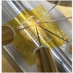
In this work, we successfully used wet etching to remove Si substrate and transferred AlGaN/GaN HEMTs arrays with LG= 2 μm to the flexible Kapton tape. The area transferred of AlGaN/GaN epitaxial thin film reached to 1.2 x 1.2 cm2. The flexible HEMTs still exhibits excellent electrical properties with the Jds,max of 290 mA/mm, and the gm,max of 108 mS/mm. Furthermore, we analyzed physical mechanisms when devices under bending. Under bending, the tensile strain enhances the piezoelectric field within the AlGaN layer so that increase the 2DEG density. In the condition that flexible HEMTs are bent with radius of curvature = 0.3 cm, the Jds,max reaches to 346 mA/mm, and the gm,max achieves to 125 mS/mm. Besides, by pulse I-V measurement, we verified that the main reason for the decrease of DC characteristics is self-heating. As for the RF characteristics, we found that Si substrate removal can effectively decreases the output parasitic capacitances. Although the gm,max becomes half after transfer processes, the fT and the fmax of the flexible HEMTs still reach to 3.8 GHz and 6.5 GHz, respectively.
文章摘要:
在這項研究中,我們成功地使用濕法蝕刻去除了 Si 基板,並將閘極長度 ( LG )為 2 μm 的 AlGaN/GaN HEMT 陣列轉移到軟性 Kapton 膠片上。AlGaN/GaN磊晶薄膜的轉移面積達到1.2 x 1.2 cm2。軟性膠片上的 HEMT 仍然表現出優異的電性,最大汲極電流密度 (Jds,max) 為 290 mA/mm,互導 (gm,max) 為 108 mS/mm。此外,我們分析了軟性膠片彎曲時 HEMT的物理機制。在彎曲下,拉伸應變增強了 AlGaN 層內的壓電場,從而增加了二維電子雲 (2DEG) 密度。在軟性膠片上HEMTs以曲率半徑為 0.3 cm彎曲的情況下,最大汲極電流密度可達到346 mA/mm,互導可達到125 mS/mm。此外,通過脈衝電流-電壓 (Pulse I-V)量測,我們驗證了直流特性下降的主要原因是自熱效應所致。至於射頻特性,我們發現去除矽基板可以有效地降低輸出寄生電容。雖然互導在傳輸過程後變為一半,但軟性膠片上的 HEMT 之截止頻率 (fT) 和極大振盪 頻率 (fmax) 仍分別達到 3.8 GHz 和 6.5 GHz。
